How do you find the form factor of a full wave rectifier?
For a full wave rectifier, the RMS voltage V RMS = V m / √2 and the average Voltage, V AVG = 2 V m / π. Form factor value of full wave rectifier = ( V m / √ 2 ) / ( 2V m / π ) = π V m / 2√2 V m = 1.11. Ripple factor of rectifier
What is transformer utilization factor of full wave rectifier?
Increase in Transformer utilization factor suggests a better performance of the full wave rectifier. Efficiency of Full Wave Rectifier is defined as the ratio of the DC power available at the load to the input AC power. It is represented by the symbol – η Efficiency of a ideal Full Wave Rectifier Circuit is = 81.2%
Why do we use a full wave rectifier?
Significant power is lost while using a half-wave rectifier and is not feasible for applications that need a smooth and steady supply. For a more smooth and steady supply, we use the full wave rectifiers. In this article, we will be looking into the working and characteristics of a full wave rectifier.
What is the peak factor of full wave rectifier?
Peak factor is defined as the ratio of the peak value of the output voltage to the rms value of the output voltage. Peak inverse voltage for Full Wave Rectifier is 2Vm because the entire secondary voltage appears across the non-conducting diode.
What is the form factor in single phase full wave bridge rectifier?
Form factor (FF) is a ratio of root-mean-square value of voltage or current to it's average value. Reader must note that only half-wave rectifier with resistive load produce harmonic currents in their transformers. For instance, Digi-Key Electronics offers great range of single-phase full-wave and bridge rectifiers.
What is ripple factor formula for full wave rectifier?
Full wave rectifier: Find out Vrms and ripple factor (r) using formula for full wave rectifier with filter as: Vrms= Vrp-p/4√3 and ripple factor (r) =1/ (4√3 f RLC), where Vrp-p is peak to peak ripple voltage.
How do you calculate the form factor of a rectifier?
1:104:16Half Wave Rectifier (Form Factor) - YouTubeYouTubeStart of suggested clipEnd of suggested clipSo the form factor the form factor is equal to the V RMS. The RMS load voltage divided. By V averageMoreSo the form factor the form factor is equal to the V RMS. The RMS load voltage divided. By V average. So this is how we calculate the form factor and this is the definition.
What is form factor and Peak Factor?
The form factor of an alternating current waveform is the ratio of the RMS value to the average value. The peak factor is the peak amplitude of the waveform divided by the RMS value of the waveform. For square waveform form factor and peak factor is the same and value is one.
What form factor means?
1) In computers, the form factor is the size, configuration, or physical arrangement of a computing device. The term is commonly used in describing the size and/or arrangement of a device, acomputer case or chassis or one of its internal components such as a motherboard or a daughterboard.
What is ripple factor of full wave?
Advantages of Full Wave Rectifier The value of ripple factor in full wave rectifier is 0.482 while in half wave rectifier it is about 1.21.
What is ripple factor?
Ripple factor is defined as. The ratio of RMS value of an alternating current component in the rectified output to the average value of rectified output. The ripple factor is denoted as γ. It is a dimensionless quantity and always has a value less than unity.
Which waveform has highest form factor?
Detailed Solution. Square wave will have the highest RMS value.
What is the form factor of a wave?
In electronics or electrical engineering the form factor of an alternating current waveform (signal) is the ratio of the RMS (root mean square) value to the average value (mathematical mean of absolute values of all points on the waveform).
What is form factor and its formula?
Definition: The ratio of the root mean square value to the average value of an alternating quantity (current or voltage) is called Form Factor. The average of all the instantaneous values of current and voltage over one complete cycle is known as the average value of the alternating quantities.
What is the formula of form factor?
The ratio between RMS value and Average value of an alternating quantity (Current or Voltage) is known as Form Factor....What is Form Factor.Waveform TypeFormula for Form FactorValueFull wave rectified sine waveπ/2√21.11072073Square wave11Triangle waveform2/√31.154700543 more rows
What is a full wave rectifier?
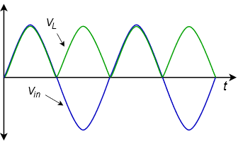
Full wave rectifiers convert both polarities of the input AC waveform to pulsating DC.
Why do we use a capacitor in full wave rectifier circuit?
A capacitor is used in the circuit to reduce the ripple factor.
What is a centre tapped full wave rectifier?
A centre tapped full wave rectifier is a type of rectifier that uses a centre tapped transformer and two diodes to convert the complete AC signal i...
Where is a full wave rectifier used?
A full wave rectifier is used in signal modulation and in electric welding.
What are the disadvantages of full wave rectifiers?
The full wave rectifiers are not suitable to use when a small voltage is required to be rectified. This is because, in a fullwave circuit, two diod...
What is the input AC supplied to a full wave rectifier?
The input AC supplied to the full wave rectifier is very high. The step-down transformer in the rectifier circuit converts the high voltage AC into low voltage AC. The anode of the centre tapped diodes is connected to the transformer’s secondary winding and connected to the load resistor. During the positive half cycle of the alternating current, the top half of the secondary winding becomes positive while the second half of the secondary winding becomes negative.
What happens to the top half of the secondary winding during the positive half cycle of the alternating current?
During the positive half cycle of the alternating current, the top half of the secondary winding becomes positive while the second half of the secondary winding becomes negative.
Why is the diode D1 reverse biased?
During the negative half cycle, the diode D 1 is reverse biased and the diode D 2 is forward biased because the top half of the secondary circuit becomes negative and the bottom half of the circuit becomes positive. Thus in a full wave rectifiers, DC voltage is obtained for both positive and negative half cycle.
What is a full wave rectifier?
Full-wave rectifiers are kind of rectifiers that converts ac to dc that is alternating current to direct current. This type of rectifier allows both halves of the ac input voltage to pass through the circuit. Two diodes are necessary to make a full-wave rectifier.
What is the efficiency of a full wave rectifier?
Efficiency of Full Wave Rectifier is defined as the ratio of the DC power available at the load to the input AC power. It is represented by the symbol – η
What is PIV in a diode?
It is defined as the maximum reverse bias voltage applied across the diode before entering the Zenner Region or Breakdown Region.
What is ripple factor?
Ripple factor is given as the RMS (Root Means Square) Value of AC Component to the Average value of the output. The output current consists of both the AC and DC components. The ripple factor measures the percentage of AC components present in the rectified output. The symbol represents the ripple factor – γ
What is the process of converting a voltage to a current?
Rectification. Rectification is the electrical process to convert an alternating current (or voltage) to direct current (or voltage). A rectifier is a device that has a low resistance to current in one direction and higher resistance in another order.
Is D1 a half wave rectifier?
As both halves of the cycle passed through the circuit , this is known as a Half wave rectifier.
Does diode D1 conduct current?
For the next half of the process, diode D1 is at revere biased, and diode D2 is forward biased. So, diode D1 does not conduct the current while D2 does for this half of the input cycle. The load current is the sum of current from diode D1 and diode D2 from both the input voltage cycles.
Centre Tap Full Wave Rectifier
The circuit of centre tap full wave rectifier consists of following main components −
Working of Centre – Tap FWR Circuit
During the positive half cycle of input AC voltage, the end A of secondary winding becomes positive and the end B negative. This makes the diode D1 forward biased (acts as closed switch) and diode D2 reverse biased (acts as open switch). Therefore, current flows through the load (RL) from P to O.
Negative Half Cycle
During the negative half cycle of input AC supply, the end B of secondary winding becomes positive and the end A negative. This makes the diode D2 forward biased (acts like closed switch) and the diode D1 reverse biased (acts as open switch).
Output Frequency of Centre – Tap FWR
The output frequency is twice the input frequency. Since the input supply is sine wave that repeats every 2π radians. The output of FWR is pulsating DC that repeats the same pattern as input AC twice every 2π radians.
Full Wave Bridge Rectifier
The full wave bridge rectifier eliminates the need of centre tapped transformer. It contains four diodes connected to form bridge.
Circuit Diagram of Bridge FWR
The circuit of full wave bridge rectifier consists of following main components −
Working of Bridge FWR
During positive half cycle, the end A of secondary winding becomes positive and the end B negative. This makes diodes D1 and D3 forward biased (acts like closed switch) and diodes D2 and D4 reverse biased (acts like open switch). The current flows from A to B through diode D1, load RL and diode D3.